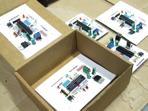
This is a fully functional version of the Arduino. We eliminated the PCB and use paper and cardboard as support and the result is.. the PAPERduino 😀
This is the the first version of the layout design, next we will try more designs, and other materials. You just need to print the top and the bottom layouts, and glue them to any kind of support you want. We hope that you start making your own boards. If you do, please share your photos with us, we would love to see them 😉
There is no USB direct connection, so to program the paperduino you will need some kind of FTDI cable or adapter. One of this products will be fine:
FTDI cable from Adafruit Industries
FTDI adapter from Sparkfun
Components list:
1 x 7805 Voltage regulator
2 x LEDs (different colors)
2 x 560 Ohm resistors (between 220oHm and 1K)
1 x 10k Ohm resistor
2 x 100 uF capacitors
1x 16 MHz clock crystal
2 x 22 pF capacitors
1 x 0.01 uF capacitor
1 x button
1 x Atmel ATMega168
1 x socket 28 pin
Female and Male headers

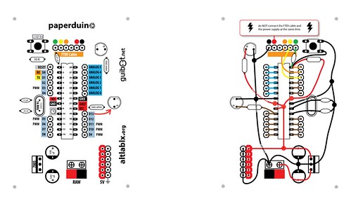
Instructions:
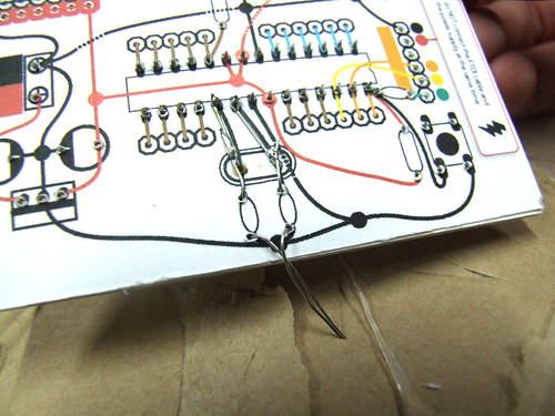
Use a needle to puncture the holes for your components.
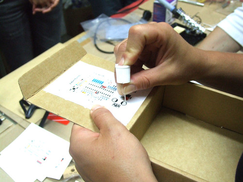
Don’t rush, place one component after another and do all the solder work carefully.
Follow the connection lines.
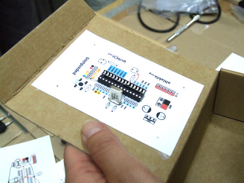
And this should be the final look of your paperduino connections.


